
理解AXI Quad Serial Peripheral Interface(SPI) IP核
在使用MicroBlaze過程中,呼叫了此IP,所以有必須仔細學習下;
名詞:
XIP: eXecute In Place
Motorola M68HC11
支援特性:
*可配置的AXI4介面
*支援對DRR/DTR FIFO的突發操作;
*支援可配置的XIP模式操作;
*支援AXI4-Lite或者AXI4介面連線的32bit Slave;
*支援可配置的SPI模式:標準、雙、四模式;
*可程式設計的SPI時鐘相位和極性;
*可配置的FIFO深度,16、256深度;對XIP模式只支援64深度;
*Configurable slave Memories in dual and quad modes are: Mixed,Micro,Winbond,and Spansion;
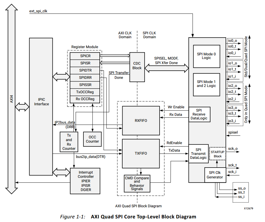

*AXI 介面選項:
XIP 模式: 使能AXI4 和 AXI4-Lite介面,地址模式可以選擇24bit和32bit;
Performance 模式:使能AXI4介面;使用AXI4介面可以在核的傳送和接收FIFO地址處啟用突發功能。當不使能performance模式時,AXI4-Lite將被使用。
*SPI 選項
模式可以選擇: standard/dual/quad
Transacton Width: 8/16/32
頻率比率:2~2048, 代表了SPI的sck = ext_spi_clk/ratio ;
NO. of Slave: 代表了slave的個數;1~32;
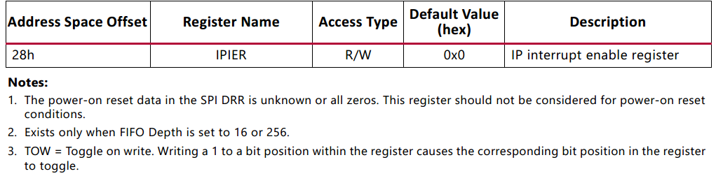
*暫存器:
AXI4-Lite寫訪問暫存器由32位AXI寫資料(* _wdata)訊號更新,不受AXI寫資料選通(* _wstrb)訊號的影響。對於寫入,AXI寫地址有效(* _awvalid)和AXI寫資料有效(* _wvalid)訊號需要同時有效。
表2-3顯示了適用的暫存器集,無論是否使能Performance Mode,或禁止XIP模式。應單獨訪問某些AXI Quad SPI核心暫存器。這些暫存器是可配置的,可通過AXI4-Lite介面或AXI4介面(增強模式)訪問。 所有暫存器都以32位的形式訪問。
如果訪問不存在的暫存器,它們將返回OKAY響應。 這些暫存器的讀取返回0,寫入沒有任何影響。
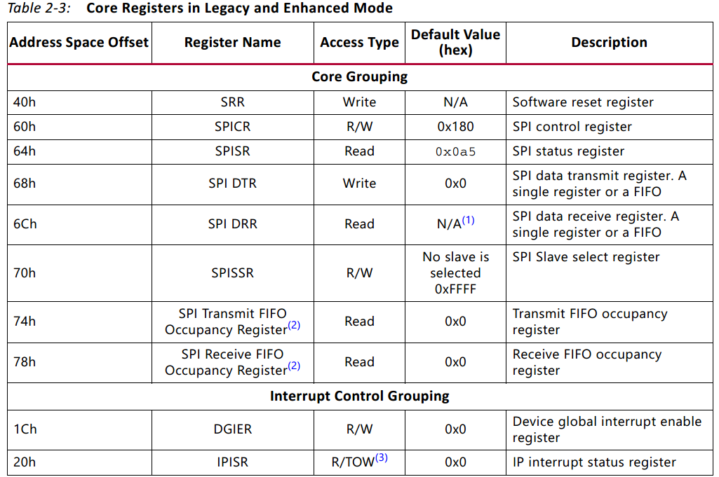
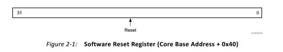
*SPISRR: 寫入0xA,進行軟體復位;
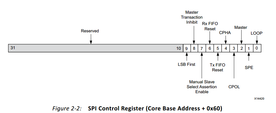
*SPICR
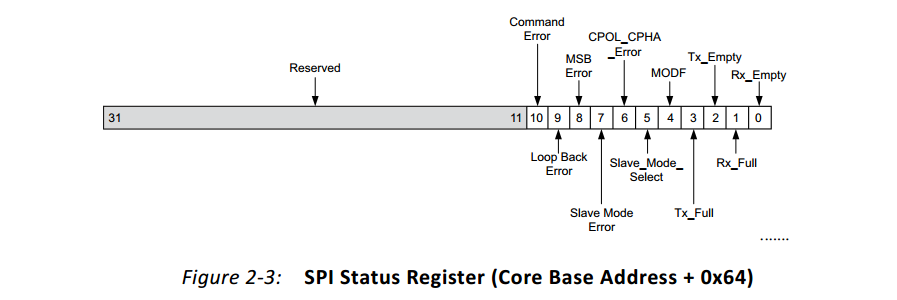
*SPISR
*SPI DTR:
After the SPE bit is set to 1 in master mode or spisel is active in the slave mode,the data is transferred from the SPI DTR to the shift register. 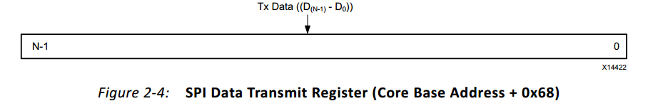
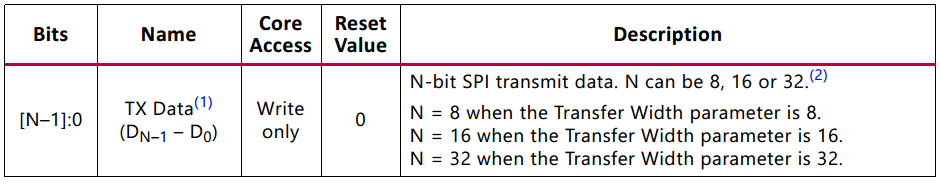
1. DN-1位始終表示MSB位,與LSB優先或MSB優先傳輸選擇無關。 當傳輸寬度引數為8或16時,未使用的高位((AXI資料寬度-1)到N)被保留。
2.在標準SPI模式下,根據核心配置,該暫存器的寬度可以是8或16或32。 在雙通道或四通道SPI模式下,該暫存器為8位寬。
* 程式設計順序:
寫使能命令順序:
1.通過置位SPICR(60h)的主禁止位來禁用主事務,並通過SPICR復位RX和TX FIFO。
示例:將0x1E6寫入SPICR
2.通過將0x06寫入SPIDTR來發出write enable命令。
3.通過向SPISSR(70h)寫入0x00來發出晶片選擇。
4.通過置低SPICR主禁止位來使能主事務。
5.通過將0x01寫入SPISSR來置低片選。
6.通過置位SPICR主禁止位來禁用主事務。
Erase Command Sequence
1. Reset RX and TX FIFOs through SPICR.
2. Issue sector erase command (a) into SPIDTR to erase any specific sector followed by the flash sector address or issue the bulk erase command (a) to erase the entire flash
followed by the flash base address.
Example: Write 0xD8 to SPIDTR
3. Issue chip select by writing 0x00 to SPISSR.
4. Enable master transaction by deasserting the SPICR master inhibit bit.
5. Deassert chip select by writing 0x01 to SPISSR.
6. Disable master transaction by asserting the SPICR master inhibit bit.
Write Data Command Sequence
1. Reset RX and TX FIFOs through SPICR.
2. Issue the write data command(a) (b) into SPIDTR, to write data into any specific sector
followed by the flash sector address.
3. Fill SPIDTR with the data to be written to flash; the maximum data size depends upon
the configured QSPI FIFO size.
4. Issue chip select by writing 0x00 to SPISSR.
5. Enable master transaction by deasserting the SPICR master inhibit bit.
6. Deassert chip select by writing 0x01 to SPISSR.
7. Disable master transaction by asserting the SPICR master inhibit bit.
Read Data Command Sequence
1. Reset RX and TX FIFOs through SPICR.
2. Issue the read data command (a) (b) into SPIDTR to read data from any specific sector
followed by the flash sector address.
3. Fill SPIDTR with the dummy data to read required data from the flash.
4. Issue chip select by writing 0x00 to SPISSR(70h).
5. Enable master transaction by deasserting the SPICR master inhibit bit.
6. Deassert chip select by writing 0x01 to SPISSR.
7. Disable master transaction by asserting SPICR master inhibit bit
8. Read SPIDRR, to get the Read data that is received from the SPI bus.
a.Refer to the respective SPI slave (flash) data sheet to know which commands to issue.
b.Write/Read commands vary with respect to the mode (Standard/Dual/Quad) used.